“Every great and deep difficulty bears in itself its own solution. It forces us to change our thinking in order to find it.” – Niels Bohr
- Mechanics: Light-assisted control, sensing, and manufacturing
- Materials: Plasmonics, metamaterials, and 2D materials
- Physics: Nonlinear, quantum, and topological photonics
- Chemistry: Photon-induced chem/med/bio-synthesis
Lán Lab’s research aims to gain a fundamental understanding of mechanics, materials, physics, and chemistry by studying photon-matter interactions at the small scale (micro, nano, molecular, and atomic). In particular, we are interested in addressing two categories of problems centered on either photons or matter. For the former, we tailor the generation, manipulation, and detection of classical and quantum light that could readily find applications in lasing, imaging, and sensing. For the latter, we utilize light to probe, program, and process natural and engineered materials for energy conversion, chemical synthesis, and clinical therapeutics. Part of the ongoing topics is illustrated in the following diagram, primarily drawing on three intriguing platforms: metamaterials, plasmonic structures, and two-dimensional (2D) materials. Several review articles are listed below to provide a basic understanding for those interested in the topics.

Research Topics at the Lán Laboratory
General Reading of Review Articles: Plasmonics – Nat. Photonics (2010); Metamaterials – Chem. Soc. Rev. (2011); Metasurfaces – Nat. Materials (2014); 2D Material Nanophotonics – Nat. Photonics (2014)
Review Articles from Lán Laboratory: Reciprocal Quantum Electrodynamics – Nanophotonics (2026); Chiral Metamaterials – Journal of Nanophotonics (2022); Photonic Environments – Nanophotonics (2021); 2D Black Phosphorus – Adv. in Optics and Photonics (2016)
METAMATERIALS
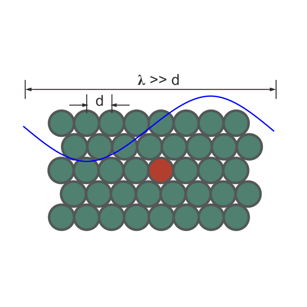
The discovery of new materials or new technologies designates a new era, for instance, the Bronze Age and the Iron Age. At the turn of this century, a new technology emerged to design materials by artificially arranging structures at a subwavelength scale. Instead of obtaining material properties by chemical compositions, this new technology relies more on geometrical designs that are readily achievable through modern semiconductor fabrication facilities. As a result, this technology has considerably extended materials space beyond the scope of natural materials, and it is named metamaterial (from the Greek word μετά meta, meaning “beyond”). Exploring these areas is of great importance for both fundamental physics and practical applications. We are particularly interested in this exciting frontier in optics and photonics. For example, we have applied a thin metamaterial to enable augmented reality on contact lenses towards dramatically reduced device footprint. With optical functionalities by design, it is arguably safe to say that photonics enters a new era named “metaphotonics.”
Nature Comm. 13 (2022), ACS Photonics 6 (2019), Nano Letters 17 (2017), Nature Comm. 8 (2017), Advanced Materials 27 (2015), Advanced Materials 26 (2014), Nano Letters 14 (2014)
PLASMONIC STRUCTURES
For a scientist, nothing is more exciting than contributing to human knowledge by finding and breaking a limit. One such limit in optics is the “diffraction limit,” which indicates that it is impossible to distinguish two objects with a distance smaller than half of the optical wavelength. Excluding super-resolution microscopy playing with the time, a possible solution is to use plasmonics on the surfaces of metals (typically gold and silver) by harvesting the near-field momenta. Unfortunately, like eating fish while dealing with the fishbone, the plasmonics will need to deal with the Ohmic loss of metals. Many applications tend to live with it, and they look at the bright side that the loss is not necessarily harmful. We are optimistic about plasmonics for recognizing the conventional role of a plasmonic metal as a conductor to conduct electric signals. Hence, the plasmonic device can simultaneously have dual optical and electrical functionalities, which is promising in nanoscale plasmonic circuitry that potentially extends Moore’s law governing modern electronics based on semiconductors. We have found some applications in nonlinear optics, plasmoelectronics, desalination, and energy conversion.
Desalination 532 (2022), Advanced Composites and Hybrid Materials (2022), Laser & Pho. Rev. 11 (2017), Nano Letters 16 (2016), Nature Materials 14 (2015), Nature Comm. 5 (2014)
2D MATERIALS
The strong in-plane bonding and relatively weak out-of-plane van der Waals forces have enabled exfoliating layered 2D materials down to only one or a few atoms thin. At this atomic scale, many exotic physics and phenomena emerge. We are interested in the fundamental study of photon-matter interactions and related quantum information science in 2D materials. A critical factor in advancing this research field is to modulate material properties beyond what they traditionally offer. Rather than modifying 2D materials directly, we surround them with an engineered electromagnetic environment or meta-environment. We investigate local and topological effects in both weak and strong coupling regimes. For instance, we utilized photonic crystals that support bound states in the continuum (BICs) to demonstrate coherent, directional emission from dark excitons otherwise optically forbidden. We also translate and explore 2D materials for future technologies with a small device scale, fast operating speed, and low energy consumption.
Nature Comm. 13 (2022), Nature Comm. 12 (2021), Nanophotonics 10 (2021), ACS Nano 14 (2020), Nano Letters 20 (2020), Advances in Optics and Photonics 8 (2016), ACS Photonics 3 (2016)
ARCHIVED PROJECTS
Ⅲ: Monolithic Full-Stokes Polarimeter
The ability to detect the full-Stokes polarization of light is vital for a variety of applications that often require complex and bulky optical systems. Here, we report an on-chip polarimeter comprising four metasurface-integrated graphene–silicon photodetectors. The geometric chirality and anisotropy of the metasurfaces result in circular and linear polarization-resolved photoresponses, from which the full-Stokes parameters, including the intensity, orientation, and ellipticity of arbitrarily polarized incident infrared light (1550 nm), can be obtained. The design presents an ultracompact architecture while excluding the standard bulky optical components and structural redundancy.
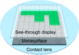
Ⅱ: Augmented Reality on Contact Lenses
Augmented reality (AR) has the potential to revolutionize the way in which information is presented by overlaying virtual information onto a person’s direct view of their real-time surroundings. By placing the display on the surface of the eye, a contact lens display (CLD) provides a versatile solution for compact AR. However, an unaided human eye cannot visualize patterns on the CLD simply because of the limited accommodation of the eye. Here, we introduce a holographic display technology that casts virtual information directly to the retina so that the eye sees it while maintaining the visualization of the real world intact.
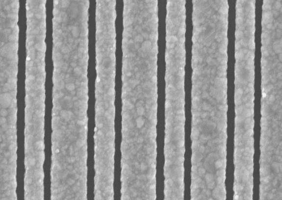
Ⅰ: Plasmonic Bound States in the Continuum
Due to the unique ability of nanostructured metals to confine and enhance light waves along with metal-dielectric interfaces, plasmonics has enabled unprecedented flexibility in manipulating light at the deep-subwavelength scale. To the spectral behavior of plasmonic resonances, the spectral location of resonance can be tailored with relative ease, while the control over the spectral linewidth represents a more daunting task. We introduce a one-dimensional plasmonic crystal with alternative strips in each unit cell (diatomic), which leads to unusually sharp and controllable resonance features. We attribute the controllable linewidth to the induced asymmetry that supports an interference-induced dark state in quantum mechanics or a bound state in the continuum (BIC).